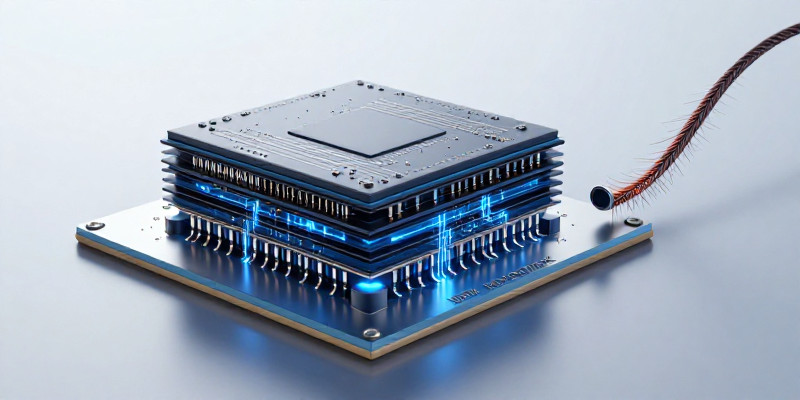
On 25 June 2026, IBM announced that it had created the world's first sub-1-nanometer transistor technology. The breakthrough uses what IBM calls "nanostack" transistors, a new way of building chips that pushes past the limits of traditional silicon manufacturing.
To understand why this matters, a little context helps. For decades, chipmakers have been shrinking transistors to make computers faster and more energy-efficient. The industry standard is now around 2 to 3 nanometers. Going below 1 nanometer was long considered a physical boundary that might take years to break. IBM just broke it.
For AI specifically, this could be transformative. Training and running large models requires enormous amounts of computing, and that computing needs chips. Smaller, more efficient transistors mean more processing power in the same physical space and with less electricity. In a world where AI power demands are straining grids and budgets, this kind of efficiency leap is exactly what the industry needs.
The technology is not in products yet. Turning a lab breakthrough into factory-ready manufacturing takes years and requires partnerships with chipmakers like Samsung or Intel. But the research proves it can be done, and that changes the roadmap for everyone.
IBM says the nanostack approach could either double chip performance at the same power or cut power use in half for the same performance. For data centers running thousands of AI workloads around the clock, that would be a game-changer. The race to make it real is now on.